


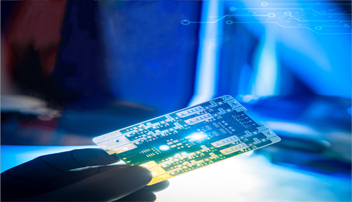
The proper PCB Panel design of a panel is crucial to guarantee the production of error-free PCBs. A panel typically contains multiple PCBs arranged in an optimal manner. Panelization offers various benefits such as time and cost-effective production, standardization, and increased protection for each individual circuit board. Panelizing circuit boards saves time and increases efficiency by processing multiple boards simultaneously instead of individually. Panel assembly can be either homogeneous or heterogeneous. In a homogenous assembly, the panel comprises only one type of circuit board. Conversely, a heterogenous assembly contains a combination of different standard circuit boards in a specific ratio.
To achieve a successful and cost-effective design of the PCB panel, it is crucial to adhere to specific guidelines:
Size of the Panel:
When designing a PCB panel, size must be considered for effective handling by machines like pick-and-place or AOI. Panels less than 2 inches may cause problems with machines, but can be fixed with extra PCBs or free space around the edges. Note the maximum panel dimensions, typically 12" x 18" (305 mm x 460 mm).
Form of the panel:
For irregularly shaped PCBs, it's important to create a handling edge. This is because automated machines like milling machines and saws are designed to work with standard, geometric shapes. A handling edge provides a reference point for machines to handle and manipulate PCBs during manufacturing. This helps ensure the accuracy and precision of the finished product.
Margin for the panel handling:
Leaving a narrow strip of free space around the edges ensures safe & secure transportation of panels. The recommended width for this strip depends on the type of PCB structure being transported. For single-sided or double-sided structures, a minimum edge width of 12.5 mm is sufficient. However, for multilayer boards, a wider edge of 25 mm is necessary to provide additional support and stability during transportation. This precaution protects the board during transit from potential damage caused by external impacts or forces.
Distance between PCBs:
The distance between individual circuit boards during the manufacturing process depends on the specific separation method being used. Laser de-paneling enables closer board spacing, usually just a few hundred micrometers. When milling is used to separate boards, a 2-3 mm distance must be maintained between them. Laser de-paneling is a non-contact process that can separate boards close to each other without damage.
Distance between cutting edge and components:
Maintain distance between the cutting edge and mounted components when cutting PCBs in manufacturing. Required distance depends on component height to avoid damage. The appropriate distance may vary depending on the specific cutting method and tools being used. Contact-based cutting methods require operators to maintain a greater distance to avoid damaging or knocking off components.
Cutting Process:
Preparing the PCB panel Design according to the specific cutting method being used is an important step in the manufacturing process. One such method is the use of breakout-tabs, which involves adding tabs to the panel to facilitate separation of the individual boards after the cutting process. By preparing the panel in advance with these tabs, manufacturers can increase the speed and efficiency of the cutting process, ultimately reducing the overall throughput time. The cutting method should be given careful consideration for each panel to ensure the highest quality and most efficient production.
PCB Power Market recognizes the challenges and varied requirements faced by designers and innovators on a daily basis. To meet their unique needs, we provide a flexible solution with a "No minimum buys" policy, allowing customers to order precisely what they need. Our commitment to customer convenience extends beyond flexible ordering, as we provide fast turnaround times for delivery across the USA. We understand that time is of the essence, and our streamlined process ensures that our customers receive their orders in a timely and efficient manner without any inconvenience. At PCB Power Market, our goal is to support our customers with reliable, hassle-free service that helps them achieve their objectives.
Original Source: https://mrguestposting.com/pcb-panel-design-guidelines-for-trouble-free-product-manufacturing/


Printed Circuit Board (PCB) Inspection Equipment research report includes specific segments by region (country), by manufacturers, by Type and by Application.
Each type provides information about the production during the forecast period of 2016 to 2027. by Application segment also provides consumption during the forecast period of 2016 to 2027.
Understanding the segments helps in identifying the importance of different factors that aid the market growth.
Download FREE Sample of this Report @ https://www.grandresearchstore.com/report-sample/global-printed-circuit-board-inspection-equipment-2021-659Segment by TypeAutomatic Optical Inspection (AOI)Automatic X-Ray Inspection (AXI)Segment by ApplicationCommercial Electronics IndustryIndustrial Electronics IndustryAutomotive IndustryBy CompanyGardienManncorpNordsonOMRONVision EngineeringBrukerGlenbrook TechnologiesHB TechnologyKohYoung TechnologyMirtecSAKITRIProduction by RegionNorth AmericaEuropeChinaJapanConsumption by RegionNorth AmericaU.S.CanadaEuropeGermanyFranceU.K.ItalyRussiaAsia-PacificChinaJapanSouth KoreaIndiaAustraliaTaiwanIndonesiaThailandMalaysiaPhilippinesVietnamLatin AmericaMexicoBrazilArgentinaMiddle East & AfricaTurkeySaudi ArabiaU.A.EGet the Complete Report & TOC @ https://www.grandresearchstore.com/manufacturing-and-construction/global-printed-circuit-board-inspection-equipment-2021-659Table of content1 Printed Circuit Board (PCB) Inspection Equipment Market Overview1.1 Product Overview and Scope of Printed Circuit Board (PCB) Inspection Equipment1.2 Printed Circuit Board (PCB) Inspection Equipment Segment by Type1.2.1 Global Printed Circuit Board (PCB) Inspection Equipment Market Size Growth Rate Analysis by Type 2021 VS 20271.2.2 Automatic Optical Inspection (AOI)1.2.3 Automatic X-Ray Inspection (AXI)1.3 Printed Circuit Board (PCB) Inspection Equipment Segment by Application1.3.1 Global Printed Circuit Board (PCB) Inspection Equipment Consumption Comparison by Application: 2016 VS 2021 VS 20271.3.2 Commercial Electronics Industry1.3.3 Industrial Electronics Industry1.3.4 Automotive Industry1.4 Global Market Growth Prospects1.4.1 Global Printed Circuit Board (PCB) Inspection Equipment Revenue Estimates and Forecasts (2016-2027)1.4.2 Global Printed Circuit Board (PCB) Inspection Equipment Production Estimates and Forecasts (2016-2027)1.5 Global Printed Circuit Board (PCB) Inspection Equipment Market by Region1.5.1 Global Printed Circuit Board (PCB) Inspection Equipment Market Size Estimates and Forecasts by Region: 2016 VS 2021 VS 20271.5.2 North America Printed Circuit Board (PCB) Inspection Equipment Estimates and Forecasts (2016-2027)1.5.3 Europe Printed Circuit Board (PCB) Inspection Equipment Estimates and Forecasts (201If You Have Any Question Related To This Report Contact Us @ https://www.grandresearchstore.com/enquire-now/global-printed-circuit-board-inspection-equipment-2021-659CONTACT US:276 5th Avenue, New York, NY 10001, United StatesInternational: +1(646)-781-7170 / +91 8087042414Email: [email protected] Us On linkedin :- https://www.linkedin.com/company/grand-research-store


